The size of the U.S. Semiconductor Plasma Dicing Tape Market was estimated at USD 0.23 billion in 2024 and is expected to increase at a compound annual growth rate (CAGR) of 8.91% from 2025 to 2032, reaching USD 0.45 billion.
Austin, Nov. 03, 2025 (GLOBE NEWSWIRE) — Semiconductor Plasma Dicing Tape Market Size & Growth Insights:
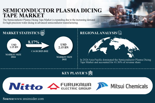
According to the SNS Insider,“The Semiconductor Plasma Dicing Tape Market size was worth USD 1.15 Billion in 2024 and is projected to reach USD 2.15 Billion by 2032, growing at a CAGR of 8.17% during 2025-2032.”
Rising Demand for High-Precision Wafer Dicing in Advanced Semiconductor Manufacturing
While the use of UV-curable and high-adhesion tapes increases wafer yield and decreases damage, the market is pushed by the growing manufacturing of MEMS, LEDs, and 3D ICs that require precision dicing. Demand is fueled by the expansion of semiconductor production and packaging facilities, while technological developments in tape materials improve dependability and efficiency. Further bolstering market expansion is the increased focus on high-quality, reasonably priced manufacturing.
Improved performance is provided by the creation of high-adhesion, UV-curable, and environmentally friendly tapes, and their use in 3D ICs, MEMS, and LED devices is growing quickly. Innovation is fueled by partnerships between semiconductor businesses and tape makers, while integration with automated dicing systems improves efficiency and scalability.
Get a Sample Report of Semiconductor Plasma Dicing Tape Market Forecast @ https://www.snsinsider.com/sample-request/8441

Leading Market Players with their Product Listed in this Report are:
- Nitto Denko Corporation
- Furukawa Electric Co., Ltd.
- Mitsui Chemicals, Inc.
- LINTEC Corporation
- Denka Company Limited
- Sumitomo Bakelite Co., Ltd.
- AI Technology, Inc.
- Pantech Tape Co., Ltd.
- Mitsubishi Chemical Corporation
- Ultron Systems, Inc.
- 3M Company
- Daest Coating India Pvt. Ltd.
- Adwill (Hitachi Chemical Co., Ltd.)
- Teraoka Seisakusho Co., Ltd.
- Loadpoint Limited
- QES Group Berhad
- Sekisui Chemical Co., Ltd.
- Teraoka Seisakusho Co., Ltd.
- Shanghai Xinke Semiconductor Material Co., Ltd.
- PULS Electronic AG
Semiconductor Plasma Dicing Tape Market Report Scope:
| Report Attributes | Details |
| Market Size in 2024 | USD 1.15 Billion |
| Market Size by 2032 | USD 2.15 Billion |
| CAGR | CAGR of 8.17% From 2025 to 2032 |
| Report Scope & Coverage | Market Size, Segments Analysis, Competitive Landscape, Regional Analysis, DROC & SWOT Analysis, Forecast Outlook |
| Key Segmentation | • By Product Type (UV Release Dicing Tape, Non-UV Dicing Tape, Thermal Release Dicing Tape, and Others) • By Application (Wafer Dicing, Die Attachment, Packaging, and Others) • By Material (Polyolefin, Polyvinyl Chloride, Polyethylene Terephthalate, and Others) • By End-User (Semiconductor Manufacturers, Electronics Manufacturers, and Others) |
Purchase Single User PDF of Semiconductor Plasma Dicing Tape Market Report (20% Discount) @ https://www.snsinsider.com/checkout/8441
Key Industry Segmentation
By Product Type
UV Release Dicing Tape led the market with approximately 42.62% share in 2024 owing to its precision and reliability in wafer dicing processes. Non-UV Dicing Tape was the fastest-growing segment with a CAGR of 8.75% due to its cost-effectiveness and versatility across various wafer types.
By Application
Wafer Dicing dominated the market with around 45.23% share in 2024 as it remains the primary process for separating individual chips from semiconductor wafers. Die Attachment recorded the fastest growth with a CAGR of 8.79% due to increasing demand for advanced packaging and assembly processes.
By Material
Polyolefin led the market with approximately 51.43% share in 2024 due to its excellent adhesion, thermal stability, and compatibility with various wafer types. Polyvinyl Chloride emerged as the fastest-growing material with a CAGR of 8.80% owing to its cost-effectiveness and versatility across different production processes.
By End-User
Semiconductor Manufacturers held the largest share at about 56.21% in 2024 as they are the primary adopters for wafer dicing and high-precision packaging applications. Electronics Manufacturers were the fastest-growing end-user segment with a CAGR of 8.78% due to increasing adoption in MEMS, LED, and emerging semiconductor devices.
Regional Insights:
In 2024, Asia Pacific dominated the Semiconductor Plasma Dicing Tape Market and accounted for 41.56% of revenue share. The region’s growth is driven by the rising semiconductor manufacturing activities, increasing production of MEMS, LEDs, and 3D ICs, and expanding wafer fabrication facilities.
North America is expected to witness the fastest growth in the Semiconductor Plasma Dicing Tape Market over 2025-2032, with a projected CAGR of 9.01% due to its established semiconductor industry, high adoption of MEMS, LEDs, and 3D ICs, and advanced wafer fabrication facilities.
Do you have any specific queries or need any customized research on Semiconductor Plasma Dicing Tape Market? Submit your inquiry here @ https://www.snsinsider.com/enquiry/8441
Recent News:
- In May 2024, Nitto Denko launched its NF735 series plasma dicing tape, designed for 2.5D/3D packaging and HBM applications, featuring halogen-free composition and superior adhesion stability under deep plasma etching. The tape is now in volume production use at Samsung’s Pyeongtaek facility and selected TSMC backend lines.
- In April 2024, Furukawa Electric introduced the F-DICE™ 8000P tape, optimized for ultra-thin (≤25μm) silicon wafers used in fan-out packaging, offering 30% lower warpage and improved debonding consistency. The product is being evaluated by ASE and Amkor for integration into next-gen AI chip packaging lines.
Exclusive Sections of the Semiconductor Plasma Dicing Tape Market Report (The USPs):
- MANUFACTURING YIELD & DEFECT ANALYSIS – helps you evaluate average production yield rates and defect ratios by bonding techniques (UV-curable, acrylic, silicone-based), offering insights into process reliability and quality control efficiency.
- APPLICATION & TECHNOLOGY DEPLOYMENT TRENDS – helps you understand the adoption share of plasma dicing tape across semiconductor packaging, MEMS, and LED applications, along with its contribution to wafer size reduction and advanced 3D IC packaging growth.
- MATERIAL UTILIZATION & ECO-FRIENDLY ADOPTION METRICS – helps you track the usage ratio of UV-curable, acrylic, and silicone-based tapes and the penetration of lead-free, sustainable adhesive materials in semiconductor manufacturing.
- PERFORMANCE & RELIABILITY BENCHMARKS – helps you assess key performance indicators such as MTBF, temperature tolerance, and failure rates under environmental stress conditions like heat, humidity, and vibration.
- AUTOMATION & PROCESS OPTIMIZATION INSIGHTS – helps you identify the degree of automation across production facilities, highlighting efficiency gains from automated tape application systems over manual processes.
- ADVANCED PACKAGING INNOVATION INDEX – helps you uncover growth opportunities within next-generation wafer-level and 3D IC packaging technologies enabled by plasma dicing tape advancements.
About Us:
SNS Insider is one of the leading market research and consulting agencies that dominates the market research industry globally. Our company’s aim is to give clients the knowledge they require in order to function in changing circumstances. In order to give you current, accurate market data, consumer insights, and opinions so that you can make decisions with confidence, we employ a variety of techniques, including surveys, video talks, and focus groups around the world.
CONTACT: Contact Us:
Rohan Jadhav - Principal Consultant
Phone: +1-315 636 4242 (US) | +44- 20 3290 5010 (UK)
Disclaimer: The above press release comes to you under an arrangement with GlobeNewswire. Business Upturn takes no editorial responsibility for the same.