Wafer Inspection System Market growth is driven by rising semiconductor complexity, demand for defect-free chips, AI-powered inspection tools, and growth in 5G, IoT, and automotive electronics.
Austin, Nov. 14, 2025 (GLOBE NEWSWIRE) — Wafer Inspection System Market Size & Growth Insights:
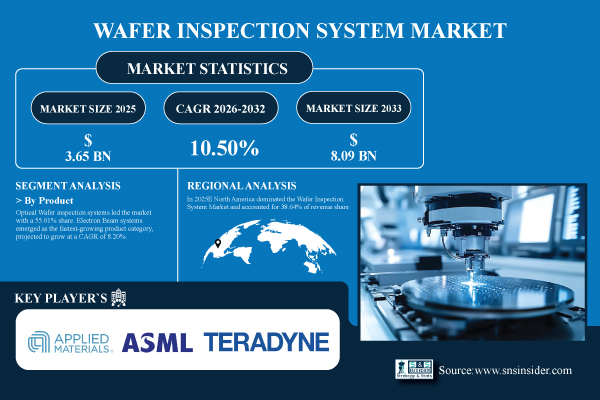
According to the SNS Insider,“The Wafer Inspection System Market size was valued at USD 3.65 Billion in 2025E and is projected to reach USD 8.09 Billion by 2033, growing at a CAGR of 10.50% during 2026-2033.”
The size of the U.S. wafer inspection system market is expected to increase at a CAGR of 10.19% from 2026 to 2033, reaching USD 2.13 billion. Growing investments in semiconductor manufacturing and domestic chip manufacture under government programs are driving the growth of the wafer inspection system market.
Surging Demand for Advanced Semiconductor Nodes to Boost Market Growth Globally
A major factor propelling the wafer inspection system market is the growing use of sophisticated semiconductor nodes like 7nm, 5nm, and beyond. Ultra-precise inspection technologies are essential for detecting micro-level flaws in devices as their complexity increases. Increasing investments in semiconductor fabrication facilities across the globe are also driving this trend, guaranteeing improved performance, increased yield, and quicker production cycles for next-generation electronics.
Get a Sample Report of Wafer Inspection System Market Forecast @ https://www.snsinsider.com/sample-request/8582

Leading Market Players with their Product Listed in this Report are:
- Applied Materials, Inc.
- KLA-Tencor Corporation
- ASML Holding N.V.
- Pacific Technology
- Teradyne Inc.
- Nanda Technologies GmbH
- Lam Research Corporation
- Hitachi High-Technologies Corporation
- Hermes Microvision, Inc.
- NXP Semiconductors
- Synopsys
- Onto Innovation Inc.
- Thermo Fisher Scientific Inc.
- JEOL Ltd.
- Nikon Metrology NV
- Camtek Ltd.
- Lasertec Corporation
- Nova Ltd.
- SCREEN Semiconductor Solutions Co., Ltd.
- BT Imaging Pty Ltd
Wafer Inspection System Market Report Scope:
| Report Attributes | Details |
| Market Size in 2025 | USD 3.65 Billion |
| Market Size by 2033 | USD 8.09 Billion |
| CAGR | CAGR of 10.50% From 2026 to 2033 |
| Report Scope & Coverage | Market Size, Segments Analysis, Competitive Landscape, Regional Analysis, DROC & SWOT Analysis, Forecast Outlook |
| Key Segmentation | • By Product (Optical Wafer and Electron Beam) • By Application (Defect Detection and Pattern Recognition) • By Type (Wafer Scanners and Wafer Probers) • By Technology (Front-End Wafer and Back-End Wafer) |
Purchase Single User PDF of Wafer Inspection System Market Report (20% Discount) @ https://www.snsinsider.com/checkout/8582
Key Industry Segmentation
By Product
Optical Wafer inspection systems led the market with a 55.01% share due to their widespread adoption, cost-effectiveness, and ability to provide rapid, high-throughput defect detection across semiconductor manufacturing processes. Electron Beam systems emerged as the fastest-growing product category, projected to grow at a CAGR of 8.20% as advanced nodes demand greater accuracy.
By Application
Defect Detection dominated the application landscape in 2025E, accounting for 60.24% of the market as semiconductor manufacturers prioritize identifying surface and sub-surface defects to improve yields and minimize manufacturing losses. Pattern Recognition is the fastest-growing application, expected to expand at a CAGR of 9.10% due to the increasing complexity of circuit designs.
By Type
Wafer Scanners held the largest market share of 58.32% in 2025E due to their essential role in inspecting entire wafers with speed and precision, making them integral to high-volume semiconductor manufacturing. Wafer Probers are the fastest-growing type segment, anticipated to grow at a CAGR of 7.50% as demand for electrical testing and validation of wafers rises, especially in smaller and more complex nodes.
By Technology
Front-End Wafer inspection commanded 62.10% market share in 2025E as it covers critical early stages of semiconductor manufacturing where precision is paramount to reduce costly downstream errors. Back-End Wafer inspection is the fastest-growing technology segment, projected to grow at a CAGR of 8.80% driven by the expansion of advanced packaging, MEMS, and heterogeneous integration.
Regional Insights:
Due to significant technological innovation and the presence of global leaders in semiconductor equipment, North America led the Wafer Inspection System Market in 2025E, accounting for 38.64% of revenue share. Local industrial growth and fab expansions are fueled by government-backed initiatives such as the CHIPS Act.
Asia Pacific is expected to witness the fastest growth in the Wafer Inspection System Market over 2026-2033, with a projected CAGR of 11.26 due to its strong base of semiconductor manufacturing hubs, especially in Taiwan, South Korea, and Japan.
Do you have any specific queries or need any customized research on Wafer Inspection System Market? Submit your inquiry here @ https://www.snsinsider.com/enquiry/8582
Recent News:
- In February 2025, Applied Materials introduced the SEMVision H20 e-beam inspection system, enhancing defect classification accuracy and throughput for advanced semiconductor nodes, accelerating yield learning and process optimization.
- In April 2025, KLA launched the 3935 and 3920 EP broadband plasma defect inspection systems, offering high sensitivity for ≤5nm logic and memory nodes, utilizing SR-DUV illumination and advanced algorithms for defect detection.
Exclusive Sections of the Wafer Inspection System Market Report (The USPs):
- INVESTMENT & R&D STATISTICS – helps you understand how leading companies are driving innovation in wafer inspection technologies through consistent R&D investments. This section covers the percentage of revenue allocated to research, patent filing trends in optical and e-beam inspection, and recent mergers, acquisitions, and strategic partnerships shaping technology advancement.
- PRODUCTION & CONSUMPTION DATA – helps you analyze the overall manufacturing landscape of wafer inspection systems by tracking annual production volumes, shipment data, and regional consumption trends. It also provides insights into capacity utilization rates, helping you identify supply-demand balances and potential bottlenecks in production efficiency.
- SUPPLY CHAIN & DISTRIBUTION ANALYSIS – helps you evaluate the strength and structure of the wafer inspection ecosystem. This includes key raw material suppliers for optics, sensors, and semiconductors, along with distribution channel breakdowns—covering direct sales, OEM alliances, and third-party distributors. It offers a holistic view of value chain resilience and delivery efficiencies.
- TECHNOLOGICAL INNOVATION INDEX – helps you track emerging advancements in inspection methodologies such as AI-based defect detection, deep UV and e-beam systems, and hybrid metrology solutions. This section highlights how next-generation technologies are improving precision, throughput, and reliability in semiconductor quality control.
- CAPACITY UTILIZATION RATES – helps you identify whether the industry is facing overcapacity or undersupply by comparing installed capacity to actual output. This aids in understanding production scalability, investment attractiveness, and operational optimization strategies of key manufacturers.
- COMPETITIVE LANDSCAPE – helps you assess the strategic positioning and market strength of leading players. It includes analysis of their R&D focus areas, product portfolios, geographic reach, and growth initiatives—enabling a comprehensive view of competitive differentiation and market share dynamics.
About Us:
SNS Insider is one of the leading market research and consulting agencies that dominates the market research industry globally. Our company’s aim is to give clients the knowledge they require in order to function in changing circumstances. In order to give you current, accurate market data, consumer insights, and opinions so that you can make decisions with confidence, we employ a variety of techniques, including surveys, video talks, and focus groups around the world.
CONTACT: Contact Us:
Rohan Jadhav - Principal Consultant
Phone: +1-315 636 4242 (US) | +44- 20 3290 5010 (UK)
Disclaimer: The above press release comes to you under an arrangement with GlobeNewswire. Business Upturn takes no editorial responsibility for the same.